
We connect chips.
You create the impossible.
We inspire the world to
rethink computing
Our technology integrates high-speed graphene photonics directly onto any electronic chip, inspiring innovators to rethink compute architectures.
Compute demand is accelerating.
Connectivity is falling behind.

Chip communication is inefficient
Standard electric connections are the bottleneck. They are too slow, generate too much heat, waste energy, throttle bandwidth, and only work over very short distances. These physical limitations drive costs up and hold the industry back.


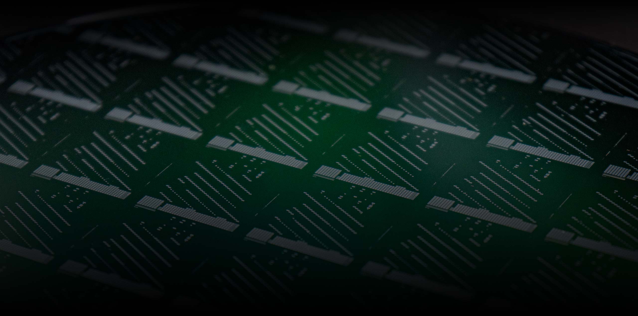
Photonics + Electronics on One Wafer
Harnessing the optical properties of graphene, we enable chips to compute with electricity and communicate with photons. This technology removes existing bandwidth limitations, allowing data centers to operate faster, cooler, and with far less energy.
Faster, More Efficient Data Transfer
Our chips convert electrical signals to optical signals instantly, reducing latency, cutting delays, and saving energy while increasing bandwidth.
Longer-Distance, High-Speed Connectivity
Optical waveguides replace copper, enabling fast, low-loss data transform.
Seamless Manufacturing Integration
CMOS-compatible processing fits into any existing chip production.
Graphene: A Single Layer That Transforms Connectivity
Graphene enables a more compact, low-power, and high-speed approach to integrating photonics and electronics at the chip level.
New Efficiency
Allows high-speed and high-efficiency broadband modulators and detectors, driving the next generation of integrated photonics.
Integration
The only material with the temperature budget, devices, and compatibility to allow BEOL integration.
Fit for Mass-Production
Works with standard CMOS fabs, ensuring scalability.
We’re moving fast!
Incorporation & Investment
Officially established by Daniel and Sebastian Schall
Raised €11.2M in VC, including public funding. Investment co-led by Vsquared and Cambium.
Build
Moved into FabOne Facility (15,000m² Fabrication space; 2,000m² office space)
Fab construction begins on a scalable pilot line for 300mm wafer technology.
Innovation
insights

What is a big enough challenge for an industry professional who wants to make an impact?
Dr. Cedric Huyghebaert shares insights on mentoring engineers, societal mechanisms, and the challenges of integrating new technology into semiconductors.

Our € 254,4 mio financing round.
Lorem ipsum dolor sit amet, consectetur adipiscing elit.
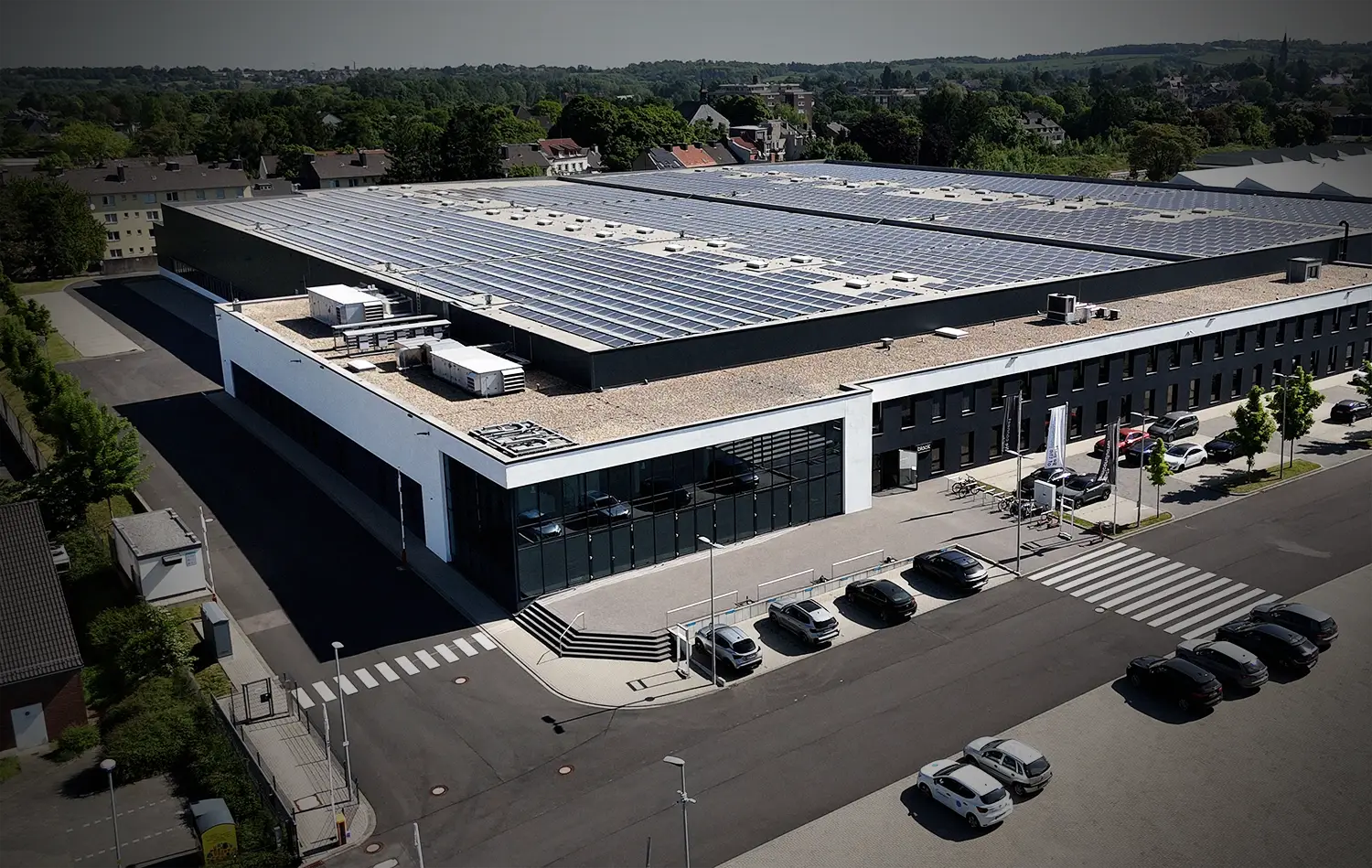
Our new headquarters, FabONE
Lorem ipsum dolor sit amet, consectetur adipiscing elit.

A change conversation
Participating in the third EU Clean Transition Dialogue.