
New material,
new possibilities.


Graphene
Black Semiconductor produces wafer-scale, single-crystal graphene with atomic precision. This material preserves superior properties and integrates seamlessly into complementary metal–oxide–semiconductor (CMOS) processes, enabling high-speed, low-power semiconductor devices.
To grow a single, continuous sheet of carbon atoms without defects, Black Semiconductor uses Chemical Vapor Deposition (CVD). Preventing the formation of graphene islands with different orientations is essential to avoid grain boundaries and a polycrystalline graphene structure. Black Semiconductor solves this challenge with an engineered substrate. Graphene grows on the substrate surface, aligning its atomic structure with the substrate’s crystal lattice in a process called epitaxial growth.
The process is controlled in such a way that only similarly oriented graphene nuclei form on the surface. By using a very low concentration of carbon precursor gas at high temperatures, the nuclei expand and cover the entire substrate, merging into a large, single-crystal graphene sheet.
This method ensures that the final material retains its electronic and mechanical properties with a minimal amount of defects or grain boundaries, which can negatively impact device performance.
The state-of-the-art process for integrating single-layer graphene onto wafers involves several steps:
- High-temperature catalytic growth
- Precise transfer to target wafers
- Interface engineering
- Dielectric capping
- CMOS-compatible contact formation
Black Semiconductor developed a proprietary process for its Integrated Graphene Photonics (IGP™) technology. Working with Tier 1 tool vendors, the company combines the most advanced semiconductor manufacturing processes with controlled interface engineering to maintain both structural quality and electrical performance.
As a result, graphene is evolving from an academic novelty into an industrial-grade material, compatible with existing complementary metal–oxide–semiconductor (CMOS) manufacturing lines and capable of meeting the reliability demands of advanced high-speed, low-power semiconductor applications.

Photodetector
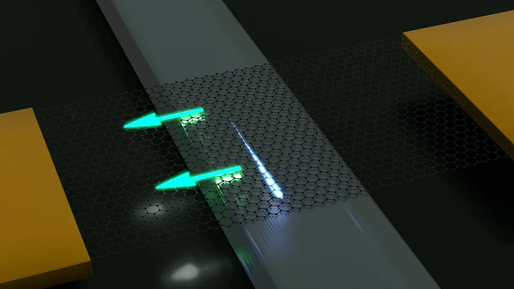
Black Semiconductor develops graphene-based photodetectors that convert optical into electrical signals with ultrafast speed. Their unique properties surpass conventional photodiodes, opening the way for next-generation optical communication.
In one approach, Black Semiconductor leverages the photo-thermoelectric (PTE) effect, which converts a temperature difference caused by absorbed light into an electrical voltage, to create graphene-based PDs.
When graphene absorbs photons, ‘hot’ carriers (electrons and holes) are created. These carriers then quickly relax and the released energy heats the surrounding carriers, creating a localized hot spot. The PTE mechanism is based on the Seebeck effect, which describes how a temperature difference across a material with an engineered non-uniform charge carrier distribution creates a voltage.
Black Semiconductor also employs the bolometric effect to create graphene-based PDs. Unlike the PTE effect, this method does not generate a voltage in response to absorbed photons. Instead, it detects light through changes in the electrical resistance of graphene caused by photo-induced heating.
As light is absorbed by the graphene layer, the resulting increase in temperature alters the carrier distribution and mobility, leading to a measurable change in resistance. By applying a constant bias (voltage or current) across the graphene and monitoring the resulting change in the electrical signal, one can infer the presence and intensity of the optical signal.
This approach does not involve the photo-generation of electron-hole pairs, as is the case with traditional photodiodes. Instead, it relies on the bolometric response – resistance modulation due to temperature change.
Graphene-based PDs are inherently fast due to their unique detection mechanism. Unlike conventional silicon or III–V PDs, which rely on photo-generated electron–hole harvesting, graphene-based devices exploit the ultrafast carrier dynamics of graphene. The fastest graphene-based PDs exhibit a bandwidth in excess of 500 GHz.
Thermalization, when absorbed light energy is converted into charge carrier heat, occurs exceptionally quickly in graphene due to strong carrier-carrier correlations in this two-dimensional (2D) material. Cooling then follows through various mechanisms, from defect-assisted supercollision in less pristine graphene to phonon-assisted processes or combinations of both.
These cooling channels are driven by the unique behavior of charge carriers in graphene, which obey the massless Dirac equation rather than the Schrödinger equation relevant for silicon and III–V semiconductors. The Kohn anomaly (a sharp dip in a material’s phonon dispersion curve at a specific wavevector, caused by strong electron–phonon interactions that efficiently screen lattice vibrations) is tightly linked to Dirac dispersion. It enhances electron–phonon interactions and accelerates phonon-assisted cooling.
The ultrafast carrier dynamics of graphene enable carrier multiplication and internal quantum efficiency above unity.
The result: unparalleled speed and sensitivity for emerging optical communication applications. Graphene, this carbon-based 2D material, continues to demonstrate exceptional properties, enabling groundbreaking performance in next-generation photodetection applications.

Modulator
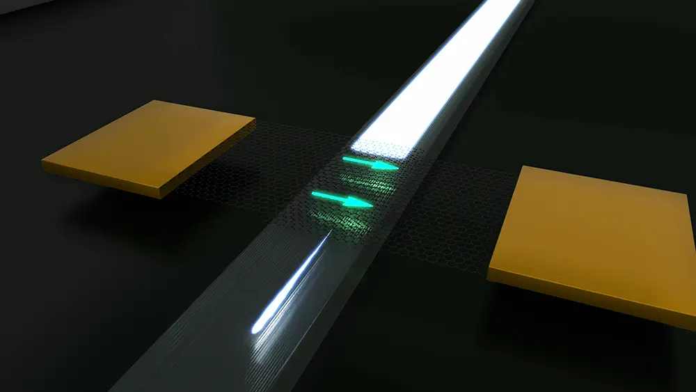
Black Semiconductor’s graphene modulators translate electrical signals into optical ones by precisely tuning light absorption. Built for speed and efficiency, they unlock scalable, high-performance optical communication beyond the limits of traditional devices.
A single layer of undoped graphene can absorb 2.3% of normal incident light. Confining light in a waveguide alongside the graphene layer increases cumulative absorption.
Graphene’s ability to change its absorption as a function of an external voltage is used to transfer electrical into optical signals. This is achieved by using two layers of graphene separated by an insulator on a waveguide. The two layers of graphene form a capacitor. The electrical signal charges or discharges the capacitor.
The resulting change in carrier concentration alters graphene’s optical absorption through Pauli blocking. This quantum mechanical principle – arising from the fact that no two fermions can occupy the same quantum state – prevents carriers from absorbing photons with a specific energy if the corresponding electronic states are filled. Discharging the capacitor restores empty states, allowing the graphene to absorb light again.
The speed of a graphene-based electro-absorption modulator is primarily limited by the resistance-capacitance (RC) time constant, which governs how quickly the device can charge and discharge through a resistor. This RC time constant is mainly determined by the graphene capacitor, the sheet resistance of the graphene, and the contact resistance between the graphene and metal contact.
The length of the capacitor along the waveguide does not affect the RC time constant, as it cancels out with the length that defines the contact resistance. However, the width of the graphene capacitor has a direct, linear influence on the RC time constant.
A smaller overlap between the two graphene sheets increases modulation speed, but this comes at the expense of modulation efficiency. In principle, this trade-off can be balanced by increasing the modulator’s length. In practice, however, this requires careful design to minimize losses and maintain optimal performance. It also depends on having stable, high-quality graphene, as the device performance is highly sensitive to the graphene band structure.

Integration
Black Semiconductor IGP™ technology integrates photonics directly onto any semiconductor chip using standard CMOS processes. By eliminating complex packaging and electrical interconnects, it removes bandwidth bottlenecks and unlocks the full potential of photonics for next-generation High Performance Compute (HPC) and AI architectures.
Black Semiconductor IGP™ technology allows both a modulator and a PD to be manufactured simultaneously from the same material: graphene. This significantly reduces the complexity of integration compared to the multi-material integration required for modulators and PDs in silicon photonics or thin-film lithium niobate (TFLN) platforms.
Black Semiconductor IGP™ technology integrates seamlessly into any chip, as all photonic fabrication steps are fully compatible with standard wafer-level semiconductor manufacturing processes. These steps are carefully engineered to prevent degradation of existing devices integrated on the wafer, enabling a CMOS-node-agnostic platform for combining photonics with any semiconductor technology.
With this capability, signals leaving the chip can operate seamlessly in either the optical or electronic domain, giving system architects the flexibility to choose the most efficient communication solution. At the same time, Black Semiconductor IGP™ technology reduces costs by eliminating the need for complex advanced packaging methods – such as hybrid bonding, through-silicon via (TSV), and ultra-thin photonic chip processing – typically required to build photonic engines.
To ensure the highest quality and reliability, Black Semiconductor exclusively uses tools and materials from Tier 1 semiconductor suppliers for graphene and photonics integration. This approach ensures full compliance with the industry’s most stringent standards and supports seamless replication across multiple semiconductor manufacturing sites.
Electronic interconnects face fundamental limits due to frequency-dependent losses, which grow exponentially with line length and signal speed. While continuous semiconductor innovation has extended their usefulness – through shorter interconnects, increased density, and techniques like chip stacking – these improvements align with Moore’s law and its corollaries, boosting information density per footprint and per watt. However, each advance brings added complexity, costs and reliance on established technology roadmaps. Without a disruptive shift, this trajectory will plateau, and incremental gains will no longer suffice to meet the performance and efficiency demands of next-generation computing.
Silicon photonics offers clear advantages for high-speed, long-distance data transfer. Once signals need to travel beyond a few millimeters or centimeters at high speeds, optical links overcome the fundamental distance-speed limitations of electronic interconnects. However, the heterogeneous integration of optical modules – such as lasers, modulators, and PDs – with traditional electronic high-performance compute (HPC) chips at scale remains a significant challenge. These scaling challenges will persist as long as optics remain isolated islands, connected to the electronic chips through the very same electrical interconnects that silicon photonics is intended to replace.
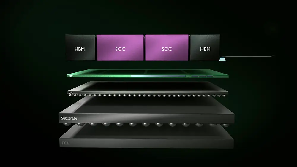
Black Semiconductor IGP™ technology overcomes the core challenge of integrating optical circuits directly onto electronics – eliminating the need for traditional electronic interconnects between compute chips and optical engines. The figure illustrates a cross-sectional view of a graphene-based chip utilizing Black Semiconductor IGP™ to seamlessly integrate photonics with electronics. The key differentiator lies in Black Semiconductor IGP™ technology’s ability to simultaneously produce photonic structures on any electronic circuit, particularly CMOS, using standard semiconductor fabrication techniques. This direct integration avoids complex, costly, and failure-prone packaging and bonding steps. By eliminating electrical interconnects altogether, Black Semiconductor IGP™ removes the fundamental source of bandwidth bottlenecks in HPC systems.
Beyond simplifying manufacturing, Black Semiconductor IGP™ technology accelerates deployment and unlocks the full performance potential of photonics for next-generation HPC and AI architectures.

Chiplet
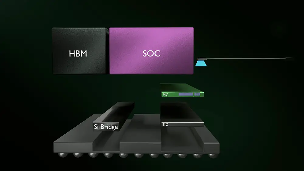
Black Semiconductor IGP™ technology integrates electronics and photonics into a single electronic-photonic chip (EPIC) independently of the CMOS node. By eliminating complex packaging and electrical interconnects, it reduces cost, improves yield, and enhances power efficiency for state-of-the-art optical interfaces.
Silicon photonics-based co-packaged optics (CPO) is emerging as the leading standard for scaling compute fabrics, addressing the bandwidth density, reach, and power limitations of copper interconnects. By enabling optical communication interfaces, CPO enhances connectivity in AI architectures.
Today’s silicon photonics CPO chips are highly complex assemblies that employ state-of-the-art packaging to integrate the electronic integrated circuit (EIC) with the photonic integrated circuit (PIC). They rely on sequential fabrication and assembly – often involving wafer-to-wafer or die-to-wafer bonding – which introduce major challenges in cost and yield. While these issues may be addressed over time, and the additional cost may be justified for certain high-value applications, integrating fiber coupling and electrical interfaces into the EIC-PIC-assembly still imposes unavoidable constraints at the packaging level.
As an alternative approach, some silicon-photonic (SiPh) technologies integrate electronic functionality directly alongside the photonics on the same chip. However, the vastly different technical requirements of electronics and photonics result in significant performance trade-offs compared to separately fabricated and bonded EIC and PIC chips. Constraints on the EIC prevent the implementation of the most advanced – and most relevant – communication protocols and interface standards. State-of-the-art protocols like Universal Chiplet Interconnect express 3.0 (UCIe 3.0) and Peripheral Component Interconnect express 6.0 (PCIe 6.0) require advanced CMOS nodes such as 5 nm or 3 nm, which are fundamentally incompatible with alongside SiPh fabrication technologies.
Black Semiconductor IGP™ technology shifts the paradigm by integrating the EIC and PIC into a single electronic-photonic chip (EPIC). By fabricating photonics directly on the most advanced CMOS nodes, Black Semiconductor IGP™ eliminates the need for complex packaging techniques like hybrid bonding, TSVs, or wafer thinning. This allows all the elements of a state-of-the-art optical interface to be consolidated into a single, compact chiplet.
This approach enables more streamlined integration of optical chiplets into packages, reducing costs and boosting yield. Removing electrical interconnects from these packages further enhances overall system power efficiency and performance.

Glass Panel Interposer
Black Semiconductor’s glass panel interposer concept dramatically expands the number of XPUs that can be connected in a single assembly. This glass interposer merges electrical connections with an extremely dense network of optical waveguides, enabling optimal data paths without the bandwidth and distance constraints of copper. By establishing a photonic interface to every XPU, direct long-distances connections become possible.
Architectures for HPC units are evolving rapidly – from a handful of XPUs in a server and tens of XPUs in a rack to clusters of thousands of XPUs spanning multiple racks. Traditional copper-based interconnects are reaching their limits, struggling to scale without incurring excessive power consumption and costs.
Black Semiconductor’s glass panel interposer concept dramatically expands the number of XPUs that can be connected in a single assembly. By establishing a photonic interface to every XPU, direct long-distances connections become possible.
This glass interposer merges electrical connections with an extremely dense network of optical waveguides, enabling optimal data paths without the bandwidth and distance constraints of copper. Black Semiconductor IGP™ technology uniquely combines active electronic-to-photonic signal conversion on every die, achieving the most efficient integration of photonics exactly where data is generated. This paradigm shift paves the way to rethink fabric architectures – enabling new scales and efficiencies previously unattainable.